Why use ceramic substrates for microelectronics?

by Sara Caron
MPT Senior Engineer
Ceramic substrates have great implications in microelectronics. First, the mechanical properties of ceramics used in microelectronics lend themselves to carriers for components. Secondly, the electrical properties of high dielectric constant and low electrical conductivity are useful in today’s electronics.
First let’s look at the mechanical properties of the ceramics used in today’s electronics: alumina (Al2O3), aluminum nitrate (AlN), and beryllium oxide (BeO). These are used in MPT processes because of their applicability to micro-electronics. They have good thermal conductivity for heat dissipation, resistance to deformation and moisture. FR-4 has a parameter called Tg (glass transition temperature), the temperature of rigid form changes to a deformable form. Ceramics do not deform with respect to temperature. Ceramics also have low thermal expansion which makes it ideal for microelectronic and microwave carriers. Note: although BeO has the greatest thermal conductivity of the ceramics, it is also highly toxic in dust form.
Other mechanical properties of ceramics for microelectronics include high fracture toughness and resistance to chemicals.
Secondly, the electrical properties of ceramics are appealing to microelectronic designers. Volume resistivity is in the order of 1011 whereas FR-4 is 106 to 10 10 and varies with moisture. The high dielectric constant of ceramics makes for smaller circuitry and is very stable compared to FR-4. Alumina has a lower dissipation or loss factor than FR-4, meaning less power is absorbed by dielectric. The loss factor is comparable to high frequency materials, but the high frequency plastic materials are susceptible to moisture and, therefore, would have more loss over moisture ranges. Ceramics do not absorb moisture and, therefore, have more stable performance. Stable capacitors are one of the many components MPT produces.
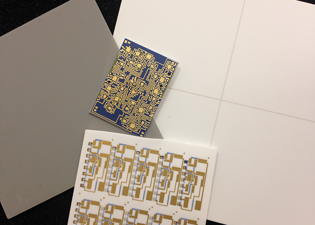
MPT has designed and assembled thick film circuits on AL2O3, AlN, and BeO with substrate thicknesses ranging from 10 mils up to 80 mils thick. Examples of circuits and parts made on the thick film process are posted at the end of this article and on our web site. These examples include capacitors, thick film resistors, hybrid circuitry, LED circuits, space based circuits, and single board computers. MPT’s engineers can design these items based on customer requirements and mechanical considerations.
References:
[1] —— http://global.kyocera.com/prdct/fc/product/pdf/material.pdf , www.kyocera.com 2017
[2] ——“MPT Thick Film Capabilities”, www.micropt.com, 2017
For further information, please contact:
Micro-Precision Technologies, Inc.
10 Manor Parkway, Suite C
Salem, NH 03079
603-893-7600
www.micropt.com
[email protected]
Certifications
MPT is MIL-PRF-38534 Class H qualified since 1998, QML-38534 listed, certified by DSCC (Defense Supply Center, Columbus, OH). MPT is AS9100D ISO 9001:2015, and ITAR registered.
